| (a) |
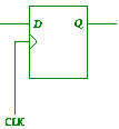
Draw the block diagram for an edge-triggered
D flip-flop.
(Must be correctly labelled to get the mark.)
|
[1] |
| (b) |
Give the excitation table for such a
flip-flop.
(All or nothing.)
|
[1] |
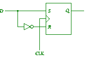
| (c) |
Show how to construct an edge-triggered
D flip-flop from an edge-triggered SR flip-flop.
(Must be correctly labelled to get the mark.)
|
[1] |
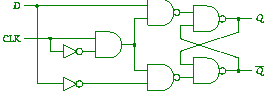
| (d) |
Show how to construct an edge-triggered
D flip-flop from ordinary logic gates (NOT, AND, OR, NAND, NOR).
(1 mark for the cross-coupled NAND gates; 1 mark for the rest of the circuit.)
|
[2] |
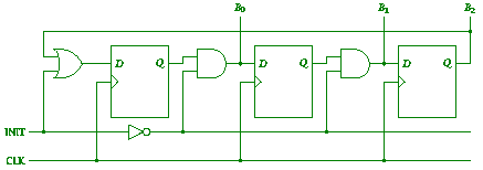
| (e) |
Show how to connect three edge-triggered
D flip-flops into a 3-bit ring counter, in which exactly one output
is high at any one time. An initialization signal should put the flip-flops
into a sensible starting state.
(1 mark for connecting the flip-flops in a loop; 1 mark for connecting the clock signal; 1 mark for implementing the initialization signal correctly; 1 mark for clear labelling.)
|
[4] |
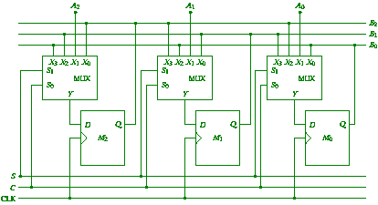
| (f) |
A 3-bit register has three 1-bit memory
cells if S is low and C is low, the cells
hold their contents unchanged; The contents of the cells are always
available on the data outputs. Design a circuit to implement such
a register, using three edge-triggered D flip-flops and three 4-to-1
multiplexors.
(1 mark for the
three memory cells and their output signals; 1 mark for the connecting
the outputs from the multiplexors to the inputs of the memory cells;
1 mark for connecting the data inputs to the multiplexors; 1 mark
for connecting the control inputs to the multiplexors; 1 mark for
labelling (including the multiplexor inputs); 1 mark for a clear diagram.
Note that other arrangements are possible; for example, S and C could
be connected to |
[6] |