|
A. Number System (5)
(a) Convert the number 40.12510 into Binary. [2]
40.12510
= 101000.0012
Guide: 1 mark for the integar part, 1 mark for the fractional part.
(b) Add together the different
number systems, ( 38 + E0416 ) and give the
answer in BCD. [3]
( 348
+ E0416) =
01
1100 [1]
1110
0000 0100 [1]
1110
0010 0000
1110
0010 00002
= E3816
=
14x256 +2x16
=
3584 + 32
=
361610
=
0011 0110 0001 0110BCD [1]
B. Logic Representation. (3)
(c) Find the Boolean expression for the switching circuit below. [1]
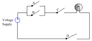
L = (A+B)CD
Guide: 1 mark for all or nothing.
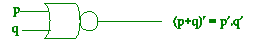
(d) Let p be statement ‘Tom speaks English’, and
q the statement ‘Tom speaks
French’. Represent the statements below using Boolean logic,
in terms of p and
q.
“Tom speaks neither English nor French” [1]
(p+q)í = pí .qí (1 mark for all or nothing)
(e) Represent the above question (d) using one Logic gate. [1]C. Boolean
Algebra. (12)
Guide: 1 mark
for NOR.
(f) Using Boolean algebra and de Morgan’s Law or otherwise prove
the property
below. [4]
A’B+AB’=[(A{AB}’)’(B{AB}’)’]’
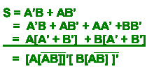
Guide:
1 mark for final answer, 3 marks for relevant working
(g) By constructing the
Karnaugh Map for the function
F(A,B,C,D) =  ( 0,1,5,13) + don’t care
  (4,14) (4,14)
find the ‘sum of products’ and ‘product of sums’.
[4]
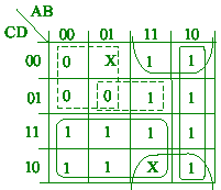
SOP
= ABí + C + ADí [1]
POS = (A + C)(Bí + C + Dí) [1]
Guide: 1 mark for the format of the Kmap, 1 mark for the entries,
1 mark for SOP, 1 mark for POS.
(h) Solve the following using Quine McClusky
the expression,
(
m0,m2, m3 m8, m9,m14,m15)
up to the prime implicants. Indicate the prime implicants clearly.
[4]
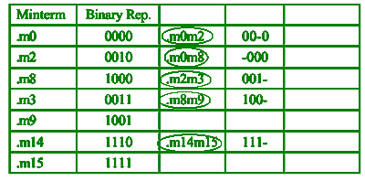
Prime implicants
in loops.
Guide: 1 mark for forming some groupings correctly; 1 mark
for giving some prime implicants correctly; and extra 1 mark for giving
all prime implicants correctly; 1 mark for layout of the table and
clarity.
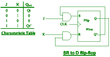
D. Sequential Circuits (8)
(i) Give the Characteristic table of a JK flip-flop and convert an
SR to a JK flip-flop.
[4]
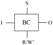
(j) A binary cell has the following connections: [4]
Guide:
1 mark for format of table and 1 mark for entries
1 mark the flip-flop connections and 1 mark for labelling
The cell acts as a single bit memory.
Its behaviour is as follows: if select
control S is low, the bit remains unchanged and the output is zero:
if S is high
and the read / write control R/W’ is high, the bit remains unchanged
and the
output O is the same as the bit; if S is high and R/W’ is low,
the bit is replaced
with the input I and the output is zero.
Design an implementation of such a cell. Hint: one implementation
can be
constructed by appropriately connecting the following components.
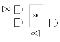
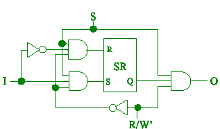
1 mark
for connecting the inputs to the SR latch via AND gates; 1 mark for
connecting S to the inputs and outputs via the AND gates; 1 mark for
connecting R/Wí to the inputs and output via the AND gates; 1 mark
for clear labelling. Alternative circuit design deserves appropriate
credit too.
E. Theory (2)
(k) Explain what is meant by the term semiconductor. [2]
A semiconductor is a material that can be
made to conduct or to insulate
two contacts, (1 mark)
depending on the voltage applied at a third contact. (1 mark)
|