| (a) | Convert the number 25510 and 80110 to binary coded decimal (BCD) notation and perform BCD addition, leaving the answer in BCD notation. Show all your working. | [4] |
| 25510 80110 _______________________ 1010 0101 0110BCD one mark for each correct conversion, plus one mark for correct binary addition.
1010 0101 0110BCD one mark for correct adjustment; no extra marks for the final answer, since there are already two marks available for conversion here, and anyone who can convert the two summands ought to be able to convert the sum from decimal notation anyway.
|
||
| (b) | Write the number -.062510 in floating point format, with a 10-bit mantissa and a 6-bit exponent, both using 2's complement representation. | [4] |
| -.062510 = -.00012 = -.1 * 2-3 = 1 100000000 * 1 11101 one mark for correct conversion to binary, one mark for correct normalisation, one mark for correct mantissa, one mark for correct exponent.
|
||
| (c) | Draw a ciruit diagrams to show how nand gates can be used to: | |
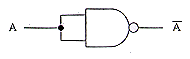
| (i) produce the output A from an input of A | [1] | |
| one mark for a
correct diagram
|
||
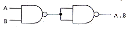
| (ii) produce the output A.B from inputs A and B | [1] | |
| one mark for a
correct diagram
|
||
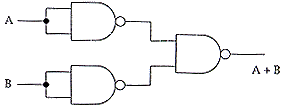
| (iii) produce the output A + B from inputs A and B | [2] | |
| Two marks for a correct diagram;
one mark out of two if the circuit produces A nor B instead of A + B
|
||
| Label the inputs and outputs in each
diagram
|
||
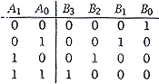
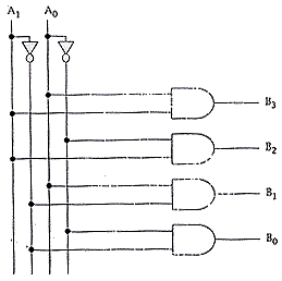
| (d) | A 2 to 4 decoder has two
inputs and four outputs:
Write fown the truth table for this decoder. Draw and label a diagram to show how it could be implemented using a combination of and and not gates: |
[4] |
one mark for correct format of table, one mark for completely correct set of entries; total two marks for the table
one mark for correct diagram, one mark for correct labelling; total two marks for the diagram
|
||
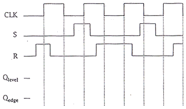
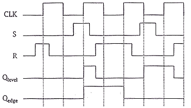
| (e) | The diagram below shows a positive
level-triggered RS flip-flop and a positive edge-triggered RS flip-flop which share the
same pair of inputs and the same clock signal.
Complete the following timing diagram to show how the two outputs Qlevel and Qedge both initially at zero, change during the four clock cycles:
|
[4] |
| one mark for each clock cycle for which both waveforms are correct. |