| (a) | Give the truth table for a half-adder.| |
[1] | ||||||||||||||||||||
|
||||||||||||||||||||||
| (b) | Express the carry and sum terms of a half-adder using NAND and NOT operations only. | [2] | ||||||||||||||||||||
| For the carry we have and for the sum we have
|
||||||||||||||||||||||
| (c) | Hence draw a circuit for a half-adder using only NAND gates. | [4] | ||||||||||||||||||||
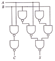
|
||||||||||||||||||||||
| (d) | Show how to construct a full-adder using two half-adders and an OR gate. | [3] | ||||||||||||||||||||
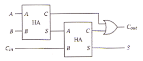
|
||||||||||||||||||||||
| (e) | Here is the truth table for a 4-to-1
multiplexor.
(Thus, when S1 = 0 and S0 = 0, the value of B is the same as that of input A0, and so on.) Explain how such a multiplexor can be used to implement an arbitrary 3-input, 1-output circuit. |
[4] | ||||||||||||||||||||
Suppose the three
inputs are X, Y, Z. Choose any two of the three inputs (says X, Y) as the selectors. For
given values of the selectors(eg X = 0, Y = 0), there are only four possible combinations
using Z for the output, namely 0, 1, Z and |
||||||||||||||||||||||
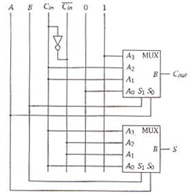
| (f) | Hence show how to implement a full-adder using two 4-to-1 multiplexors. | [6] | ||||||||||||||||||||
 |